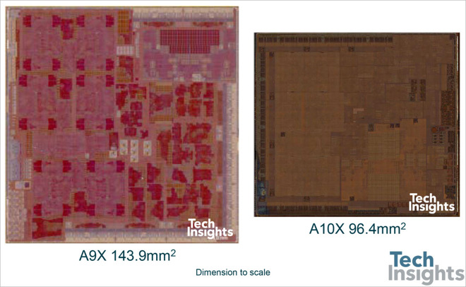
A breakdown published by Tech Insights shows the A10X Fusion processor powering Apple’s new iPad Pro is the first chip in a device to use TMSC’s FinFET 10nm chip fabrication process.

… A10X Fusion die size comes in at 96.4 square millimeters as compared to the 16nm A9X with a die size of 143.9 square millimeters. Even having the notably smaller die size, the chip has 8MB of L2 cache, three CPU cores, and a 12-cluster GPU assembly.
For comparison, the A9X in the previous iPad Pro also had a 12-cluster GPU assembly, but two CPU cores and 3MB of L2 cache. The GPU in the A10X is nearly identical to that in the A9X and A10, so it is likely still Imagination’s PowerVR technology.
The move is a bit unusual for Apple, who has historically first used a small manufacturing process for chips on the iPhone. Apple does group the A9 and A10 processor families together in its documentation.
The A10X Fusion processor debuted on June 5 as the brain behind the new 10.5-inch iPad Pro, as well as the refreshed 12.9-inch iPad Pro.
TechInsight notes that 10nm will likely be a short-lived node for TSMC, with multiple “7 nm” technologies around the corner, with a variety of other node names and node variants in between.


